진행년월: 24.08
- 이전 글
(1) 2차원 Filter : https://chonh0531.tistory.com/20
Filter - (2) FPGA에서 CNN구현
진행년월: 24.08 목차1. 배경2. 과제 정의 및 개요3. 소스코드4. 시뮬레이션 결과 1. 배경CNN 모델 중 가장 기본적인 Lenet-5 모델을 구현해보려고 합니다.메모리 등을 고려해야 하기 때문에,성능 자
chonh0531.tistory.com
목차
1. 배경
2. 과제 정의 및 개요
3. 소스코드
4. 시뮬레이션 결과
1. 배경
CNN 모델 중 가장 기본적인 Lenet-5 모델을 구현해보려고 합니다.
메모리 등을 고려해야 하기 때문에,
성능 자체를 끌어올리기보다는 구현 자체에 초점을 맞춥니다.
2. 과제 정의 및 개요

구현할 모델은 위와 같습니다.
1. CNN Python코드 작성
2. Verilog 구현용 C코드 작성
3. Verilog 코드 구현
4. 이미지 예측 정확도 평가
3. 소스코드
- Python CNN
import tensorflow as tf
from tensorflow.keras import layers, models
import numpy as np
import struct

# **1. LeNet-5 모델 정의**
def build_lenet5():
    model = models.Sequential([
        layers.Conv2D(6, (5, 5), activation='relu', input_shape=(28, 28, 1)),
        layers.AveragePooling2D((2, 2)),
        layers.Conv2D(16, (5, 5), activation='relu'),
        layers.AveragePooling2D((2, 2)),
        layers.Flatten(),
        layers.Dense(120, activation='relu'),
        layers.Dense(84, activation='relu'),
        layers.Dense(10, activation='softmax')
    ])
    return model

# **2. 데이터셋 로드 및 전처리**
def load_data():
    (x_train, y_train), (x_test, y_test) = tf.keras.datasets.mnist.load_data()
    x_train = x_train / 255.0  # Normalize to [0, 1]
    x_test = x_test / 255.0
    x_train = np.expand_dims(x_train, axis=-1)  # Add channel dimension
    x_test = np.expand_dims(x_test, axis=-1)
    return (x_train, y_train), (x_test, y_test)

# **3. 양자화 함수: 32비트를 8/11비트로 변환**
def quantize(value, bits=8, frac_bits=4):
    scale = 2 ** frac_bits
    quantized = np.round(value * scale)
    quantized = np.clip(quantized, -(2 ** (bits - 1)), 2 ** (bits - 1) - 1)
    return quantized.astype(np.int16)

# **4. 학습과 가중치 저장**
def train_and_save_weights(model, x_train, y_train, x_test, y_test, quant_bits=8, frac_bits=4):
    model.compile(optimizer='adam',
                  loss='sparse_categorical_crossentropy',
                  metrics=['accuracy'])
    model.fit(x_train, y_train, epochs=5, validation_data=(x_test, y_test))
    test_loss, test_acc = model.evaluate(x_test, y_test)
    print(f"Test Accuracy (Python): {test_acc:.4f}")

    # Save weights for FPGA implementation
    for layer in model.layers:
        if isinstance(layer, (layers.Conv2D, layers.Dense)):
            layer_weights, layer_biases = layer.get_weights()

            # 양자화된 가중치 저장
            quantized_weights = quantize(layer_weights, quant_bits, frac_bits)
            quantized_biases = quantize(layer_biases, quant_bits, frac_bits)

            # 파일 저장
            np.savetxt(f"{layer.name}_weights.txt", quantized_weights.flatten(), fmt='%d')
            np.savetxt(f"{layer.name}_biases.txt", quantized_biases, fmt='%d')

            print(f"Weights and biases for layer '{layer.name}' saved.")

    print("All layer weights and biases saved.")
    return test_acc

# **5. 테스트 데이터 저장 (Verilog 테스트벤치용)**
def save_test_data(x_test, y_test):
    (x_test, y_test) = (x_test[:1000], y_test[:1000])  # 제한된 샘플 수로 간단히 처리
    x_test_flat = x_test.reshape(x_test.shape[0], -1)  # Flatten 28x28 images to 784

    # Save test data
    np.savetxt('test_images.txt', x_test_flat, fmt='%d')  # Save as integer values (0-255)
    np.savetxt('test_labels.txt', y_test, fmt='%d')      # Save labels

    print("Test images and labels saved.")

# **Main Script**
if __name__ == "__main__":
    # Load data
    (x_train, y_train), (x_test, y_test) = load_data()

    # Build model
    model = build_lenet5()

    # Train model and save weights
    python_accuracy = train_and_save_weights(model, x_train, y_train, x_test, y_test)

    # Save test data
    save_test_data(x_test, y_test)
python으로 모델을 구성한 뒤, 학습을 진행합니다.
테스트 데이터는 MNIST 데이터를 사용하였습니다.
학습된 모델의 Weight와 Bias를 Vivado에서 Block 메모리 초기화 파일로 사용하기 위해
COE 파일로 저장합니다.
- Verilog CNN 이전 Convolution test
module cnn (
    input clk,
    input reset,
    input [7:0] t_rdata,
    output reg [9:0] t_addr,
    output reg [11:0] output_address, // Output memory address
    output reg signed [10:0] output_data, // Output write data
    output reg output_write_enable // Output write enable
);

// RAM Signals
reg [9:0] image_address;
reg [7:0] image_write_data;
wire [7:0] image_read_data;
reg image_write_enable;
wire signed [10:0] output_read_data;

// ROM Signals
reg [7:0] weight_address;
wire signed [7:0] weight_read_data;
reg [2:0] bias_address;
wire signed [7:0] bias_read_data;

// Loop Index Registers
reg [4:0] row, next_row, col, next_col;
reg [2:0] filter, next_filter, kernel_row, next_kernel_row, kernel_col, next_kernel_col;

// Additional Registers
reg [9:0] current_image_address, next_image_address;
(* use_dsp = "yes" *) reg signed [18:0] conv_sum, next_conv_sum;
reg [7:0] current_weight_address, next_weight_address;
reg [11:0] current_output_address, next_output_address;
reg signed [10:0] temp_output, next_temp_output;

// State Definitions
localparam s0 = 0, s1 = 1, s2 = 2, s3 = 3, s4 = 4, s5 = 5, s6 = 6;
reg [3:0] state, next_state;

// File Descriptor
integer fd;

// RAM Instantiation
i_ram image_ram (
    .clka(clk),
    .wea(image_write_enable),
    .addra(image_address),
    .dina(image_write_data),
    .douta(image_read_data)
);

a_ram output_ram (
    .clka(clk),
    .wea(output_write_enable),
    .addra(output_address),
    .dina(output_data),
    .douta(output_read_data)
);

// ROM Instantiation
w0_rom weight_rom (
    .clka(clk),
    .addra(weight_address),
    .douta(weight_read_data)
);

b0_rom bias_rom (
    .clka(clk),
    .addra(bias_address),
    .douta(bias_read_data)
);

// Finite State Machine (FSM)
always @ (reset, state, t_rdata, image_read_data, output_read_data, weight_read_data, bias_read_data, row, col, filter, kernel_row, kernel_col, current_image_address, conv_sum, current_weight_address, current_output_address, temp_output) begin
    // Default memory settings
    t_addr = 0;
    image_address = 0;
    image_write_data = 0;
    image_write_enable = 0;
    output_address = 0;
    output_data = 0;
    output_write_enable = 0;
    weight_address = 0;
    bias_address = 0;

    // Default register settings
    next_state = state;
    next_row = row;
    next_col = col;
    next_filter = filter;
    next_kernel_row = kernel_row;
    next_kernel_col = kernel_col;
    next_image_address = current_image_address;
    next_conv_sum = conv_sum;
    next_weight_address = current_weight_address;
    next_output_address = current_output_address;
    next_temp_output = temp_output;

    case (state)
        s0: begin
            next_state = s1;
            next_image_address = 0;
            t_addr = 0;
            next_row = 0;
            next_col = 0;
        end

        s1: begin
            image_write_data = t_rdata;
            image_address = current_image_address;
            image_write_enable = 1'b1;
            next_state = s1;
            next_col = col + 1;
            if (next_col == 28) begin
                next_col = 0;
                next_row = row + 1;
                if (next_row == 28) begin
                    next_row = 0;
                    next_state = s2;
                end
            end
            next_image_address = next_row * 28 + next_col;
            t_addr = next_image_address;
        end

        s2: begin
            next_filter = 0;
            next_row = 0;
            next_col = 0;
            next_conv_sum = 0;
            next_kernel_row = 0;
            next_kernel_col = 0;
            image_address = 0;
            weight_address = 0;
            next_state = s3;
        end

        s3: begin
            next_conv_sum = conv_sum + $signed({1'b0, image_read_data}) * weight_read_data;
            next_state = s3;
            next_kernel_col = kernel_col + 1;
            if (next_kernel_col == 5) begin
                next_kernel_col = 0;
                next_kernel_row = kernel_row + 1;
                if (next_kernel_row == 5) begin
                    next_kernel_row = 0;
                    next_state = s4;
                    bias_address = filter;
                end
            end
            next_image_address = (row + next_kernel_row) * 28 + col + next_kernel_col;
            next_weight_address = filter * 25 + next_kernel_row * 5 + next_kernel_col;
            image_address = next_image_address;
            weight_address = next_weight_address;
        end

        s4: begin
            next_temp_output = conv_sum[18:8];
            if (next_temp_output[10] == 1'b1) begin
                next_temp_output = next_temp_output + (|conv_sum[7:0]); // Round towards zero (RTZ)
            end
            next_temp_output = next_temp_output + bias_read_data;
            if (next_temp_output[10] == 1'b1) begin
                next_temp_output = 0;
            end
            next_output_address = filter * 576 + row * 24 + col;
            output_address = next_output_address;
            output_data = next_temp_output;
            output_write_enable = 1'b1;
            next_state = s3;
            next_col = col + 1;
            if (next_col == 24) begin
                next_col = 0;
                next_row = row + 1;
                if (next_row == 24) begin
                    next_row = 0;
                    next_filter = filter + 1;
                    if (next_filter == 6) begin
                        next_filter = 0;
                        next_state = s5;
                    end
                end
            end
            next_conv_sum = 0;
            next_image_address = next_row * 28 + next_col;
            next_weight_address = next_filter * 25;
            image_address = next_image_address;
            weight_address = next_weight_address;
        end

        s5: begin
            next_state = s5;
        end

        default: begin
            next_state = s0;
        end
    endcase

    if (reset == 1) begin
        next_state = s0;
        next_row = 0;
        next_col = 0;
        next_filter = 0;
        next_kernel_row = 0;
        next_kernel_col = 0;
        next_image_address = 0;
        next_conv_sum = 0;
        next_weight_address = 0;
        next_output_address = 0;
        next_temp_output = 0;
    end
end

// State update on clock edge
always @ (posedge clk) begin
    state <= next_state;
    row <= next_row;
    col <= next_col;
    filter <= next_filter;
    kernel_row <= next_kernel_row;
    kernel_col <= next_kernel_col;
    current_image_address <= next_image_address;
    conv_sum <= next_conv_sum;
    current_weight_address <= next_weight_address;
    current_output_address <= next_output_address;
    temp_output <= next_temp_output;
end

// Synthesis directives and file writing
// synthesis translate_off
always @ (posedge clk) begin
    fd = $fopen("test.txt", "a");
    if (state == s4 && output_write_enable == 1'b1) begin
        $fwrite(fd, "A[%0d][%0d][%0d] = %0d\n", filter, row, col, output_data);
    end
    if (reset == 1) begin
        fd = $fopen("test.txt", "w");
    end
    $fclose(fd);
end
// synthesis translate_on

endmodule
module tb;
    reg clk;
    reg reset;
    wire [9:0] t_addr;
    wire [7:0] t_rdata;
    wire [11:0] output_address;
    wire [10:0] output_data;
    wire output_write_enable;

    //
    // ROM instantiation
    //
    t_rom t_test (
        .clka(clk),
        .addra(t_addr),
        .douta(t_rdata)
    );

    //
    // CNN instantiation
    //
    cnn uut (
        .clk(clk),
        .reset(reset),
        .t_addr(t_addr),
        .t_rdata(t_rdata),
        .output_address(output_address),
        .output_data(output_data),
        .output_write_enable(output_write_enable)
    );

    // 100 MHz clock
    initial begin
        clk = 0;
        forever #5 clk = ~clk;
    end

    // reset
    initial begin
        reset = 0;
        #100 reset = 1;
        #100 reset = 0;
    end
endmodule
Verilog로 구현하기 전에 가장 중요한 Convolution 층을 먼저 구현하여 테스트 하였습니다.
- Verilog CNN
module lenet5_fpga (
    input clk,
    input reset,
    input [7:0] input_data,        // 8-bit quantized input pixel data
    output reg [3:0] output_class, // Predicted class (0-9)
    output reg done                // Processing done signal
);

    // Parameters
    parameter IMG_SIZE = 28;
    parameter NUM_CLASSES = 10;

    // State Machine States
    localparam IDLE = 0, LOAD_IMAGE = 1,
               CONV1 = 2, POOL1 = 3,
               CONV2 = 4, POOL2 = 5,
               FLATTEN = 6, FC1 = 7, FC2 = 8, FC3 = 9, DONE = 10;
    reg [3:0] state;

    // Layer Buffers
    reg [7:0] image [0:IMG_SIZE-1][0:IMG_SIZE-1]; // 8-bit Image Data
    reg signed [10:0] conv1_out [0:23][0:23][0:5];  // 11-bit Conv1 output
    reg signed [10:0] pool1_out [0:11][0:11][0:5];  // 11-bit Pool1 output
    reg signed [10:0] conv2_out [0:7][0:7][0:15];   // 11-bit Conv2 output
    reg signed [10:0] pool2_out [0:3][0:3][0:15];   // 11-bit Pool2 output
    reg signed [10:0] fc1_out [0:119];              // FC1 output
    reg signed [10:0] fc2_out [0:83];               // FC2 output
    reg signed [10:0] fc3_out [0:NUM_CLASSES-1];    // FC3 output

    // Flatten Buffer
    reg signed [10:0] pool2_flat [0:399]; // Flattened Pool2 Output

    // Temporary Registers
    reg signed [18:0] conv_sum; // For convolution accumulation
    reg signed [18:0] fc_sum;   // For FC accumulation
    reg signed [10:0] max_val;
    reg [3:0] max_index;
    integer i, j, k, kr, kc, c, row, col;

    // Block Memory Generators for weights and biases
    wire [7:0] conv1_weight_data;
    wire [7:0] conv2_weight_data;
    wire [7:0] fc1_weight_data;
    wire [7:0] fc2_weight_data;
    wire [7:0] fc3_weight_data;
    wire [7:0] bias_data;

    reg [15:0] conv1_weight_addr;
    reg [15:0] conv2_weight_addr;
    reg [15:0] fc1_weight_addr;
    reg [15:0] fc2_weight_addr;
    reg [15:0] fc3_weight_addr;
    reg [15:0] bias_addr;

    // Instantiate Block RAMs for weights and biases
    blk_mem_gen_conv1_weights conv1_weights_bram (
        .clka(clk),
        .wea(1'b0),
        .addra(conv1_weight_addr),
        .dina(8'b0),
        .douta(conv1_weight_data)
    );

    blk_mem_gen_conv2_weights conv2_weights_bram (
        .clka(clk),
        .wea(1'b0),
        .addra(conv2_weight_addr),
        .dina(8'b0),
        .douta(conv2_weight_data)
    );

    blk_mem_gen_fc1_weights fc1_weights_bram (
        .clka(clk),
        .wea(1'b0),
        .addra(fc1_weight_addr),
        .dina(8'b0),
        .douta(fc1_weight_data)
    );

    blk_mem_gen_fc2_weights fc2_weights_bram (
        .clka(clk),
        .wea(1'b0),
        .addra(fc2_weight_addr),
        .dina(8'b0),
        .douta(fc2_weight_data)
    );

    blk_mem_gen_fc3_weights fc3_weights_bram (
        .clka(clk),
        .wea(1'b0),
        .addra(fc3_weight_addr),
        .dina(8'b0),
        .douta(fc3_weight_data)
    );

    blk_mem_gen_bias bias_bram (
        .clka(clk),
        .wea(1'b0),
        .addra(bias_addr),
        .dina(8'b0),
        .douta(bias_data)
    );

    // FSM Logic
    always @(posedge clk or posedge reset) begin
        if (reset) begin
            state <= IDLE;
            done <= 0;
        end else begin
            case (state)
                IDLE: begin
                    done <= 0;
                    state <= LOAD_IMAGE;
                end

                LOAD_IMAGE: begin
                    row = 0;
                    col = 0;

                    // Sequentially load the image into the buffer
                    if (row < IMG_SIZE) begin
                        image[row][col] <= input_data;
                        col = col + 1;
                        if (col == IMG_SIZE) begin
                            col = 0;
                            row = row + 1;
                        end
                    end

                    // Move to the next state after loading the image
                    if (row == IMG_SIZE && col == 0) begin
                        state <= CONV1;
                    end
                end

                CONV1: begin
                    // Convolution Layer 1
                    for (i = 0; i < 24; i = i + 1) begin
                        for (j = 0; j < 24; j = j + 1) begin
                            for (k = 0; k < 6; k = k + 1) begin
                                conv1_weight_addr = k * 25; // Example address calculation
                                conv_sum = 0;
                                for (kr = 0; kr < 5; kr = kr + 1) begin
                                    for (kc = 0; kc < 5; kc = kc + 1) begin
                                        conv_sum = conv_sum +
                                                   image[i+kr][j+kc] * conv1_weight_data;
                                    end
                                end
                                conv1_out[i][j][k] <= (conv_sum + bias_data) >>> 8;
                            end
                        end
                    end
                    state <= POOL1;
                end

                POOL1: begin
                    for (i = 0; i < 12; i = i + 1) begin
                        for (j = 0; j < 12; j = j + 1) begin
                            for (k = 0; k < 6; k = k + 1) begin
                                pool1_out[i][j][k] <=
                                    (conv1_out[2*i][2*j][k] + conv1_out[2*i+1][2*j][k] +
                                     conv1_out[2*i][2*j+1][k] + conv1_out[2*i+1][2*j+1][k]) >> 2;
                            end
                        end
                    end
                    state <= CONV2;
                end

                CONV2: begin
                    for (i = 0; i < 8; i = i + 1) begin
                        for (j = 0; j < 8; j = j + 1) begin
                            for (k = 0; k < 16; k = k + 1) begin
                                conv_sum = 0;
                                for (c = 0; c < 6; c = c + 1) begin
                                    for (kr = 0; kr < 5; kr = kr + 1) begin
                                        for (kc = 0; kc < 5; kc = kc + 1) begin
                                            conv_sum = conv_sum +
                                                       (pool1_out[i+kr][j+kc][c] * conv2_weight_data);
                                        end
                                    end
                                end
                                conv2_out[i][j][k] <= (conv_sum + bias_data) >>> 8;
                            end
                        end
                    end
                    state <= POOL2;
                end

                POOL2: begin
                    for (i = 0; i < 4; i = i + 1) begin
                        for (j = 0; j < 4; j = j + 1) begin
                            for (k = 0; k < 16; k = k + 1) begin
                                pool2_out[i][j][k] <=
                                    (conv2_out[2*i][2*j][k] + conv2_out[2*i+1][2*j][k] +
                                     conv2_out[2*i][2*j+1][k] + conv2_out[2*i+1][2*j+1][k]) >> 2;
                            end
                        end
                    end
                    state <= FLATTEN;
                end

                FLATTEN: begin
                    for (i = 0; i < 400; i = i + 1) begin
                        pool2_flat[i] <= pool2_out[i/100][(i%100)/25][i%25];
                    end
                    state <= FC1;
                end

                FC1: begin
                    for (i = 0; i < 120; i = i + 1) begin
                        fc_sum = 0;
                        for (j = 0; j < 400; j = j + 1) begin
                            fc1_weight_addr = i * 400 + j;
                            fc_sum = fc_sum + pool2_flat[j] * fc1_weight_data;
                        end
                        fc1_out[i] <= (fc_sum + bias_data) >>> 8;
                    end
                    state <= FC2;
                end

                FC2: begin
                    for (i = 0; i < 84; i = i + 1) begin
                        fc_sum = 0;
                        for (j = 0; j < 120; j = j + 1) begin
                            fc2_weight_addr = i * 120 + j;
                            fc_sum = fc_sum + fc1_out[j] * fc2_weight_data;
                        end
                        fc2_out[i] <= (fc_sum + bias_data) >>> 8;
                    end
                    state <= FC3;
                end

                FC3: begin
                    max_val = -32768;
                    for (i = 0; i < NUM_CLASSES; i = i + 1) begin
                        fc_sum = 0;
                        for (j = 0; j < 84; j = j + 1) begin
                            fc3_weight_addr = i * 84 + j;
                            fc_sum = fc_sum + fc2_out[j] * fc3_weight_data;
                        end
                        fc3_out[i] <= (fc_sum + bias_data) >>> 8;
                        if (fc3_out[i] > max_val) begin
                            max_val = fc3_out[i];
                            max_index = i;
                        end
                    end
                    output_class <= max_index;
                    state <= DONE;
                end

                DONE: begin
                    done <= 1;
                end
            endcase
        end
    end
endmodule
이제 모든 층을 구현하여 코드를 구성합니다.
장비의 Memory가 충분치 않아 성능의 타협을 보고
32비트 floating point를 8비트 fixed point로 구현하였습니다.
- Verilog CNN Testbench
`timescale 1ns / 1ps

module tb_lenet5_fpga;

    // Signals
    reg clk;
    reg reset;
    reg [7:0] input_data;
    wire [3:0] output_class;
    wire done;

    // Parameters
    parameter CLK_PERIOD = 10;        // Clock period
    parameter NUM_IMAGES = 1000;     // Number of images to process
    parameter IMG_SIZE = 28;         // Image size (28x28)

    // File I/O
    integer input_file, output_file;
    integer i, j, k;
    reg [7:0] image_buffer [0:IMG_SIZE*IMG_SIZE-1]; // Buffer to hold one image

    // Instantiate DUT (Device Under Test)
    lenet5_fpga dut (
        .clk(clk),
        .reset(reset),
        .input_data(input_data),
        .output_class(output_class),
        .done(done)
    );

    // Clock generation
    always #(CLK_PERIOD / 2) clk = ~clk;

    // Testbench Logic
    initial begin
        // Initialize
        clk = 0;
        reset = 1;
        input_data = 0;

        // Open input image file
        input_file = $fopen("test_image.txt", "r");
        if (input_file == 0) begin
            $display("Error: Input image file not found!");
            $finish;
        end

        // Open output file
        output_file = $fopen("verilog_predietions.txt", "w");
        if (output_file == 0) begin
            $display("Error: Could not open output file!");
            $finish;
        end

        // Deassert reset after a few cycles
        #20 reset = 0;

        // Process NUM_IMAGES images
        for (k = 0; k < NUM_IMAGES; k = k + 1) begin
            $display("Processing image %d/%d...", k + 1, NUM_IMAGES);

            // Load one image into the buffer
            for (i = 0; i < IMG_SIZE * IMG_SIZE; i = i + 1) begin
                if (!$feof(input_file)) begin
                    $fscanf(input_file, "%d ", image_buffer[i]);
                end else begin
                    $display("Error: Unexpected end of input file!");
                    $finish;
                end
            end

            // Feed image buffer to DUT
            for (i = 0; i < IMG_SIZE; i = i + 1) begin
                for (j = 0; j < IMG_SIZE; j = j + 1) begin
                    input_data = image_buffer[i * IMG_SIZE + j];
                    #CLK_PERIOD;
                end
            end

            // Wait for done signal
            wait (done);

            // Write output class to file
            $fwrite(output_file, "%d\n", output_class);
        end

        $display("All images processed. Results saved to verilog_predictions.txt.");

        // Close files and finish simulation
        $fclose(input_file);
        $fclose(output_file);
        $finish;
    end
endmodule
이제 미리 준비한 test 데이터를 input으로 해서,
모델로 예측한 결과값들을 txt 파일로 저장합니다.
4. 시뮬레이션 결과
- Python 정확도
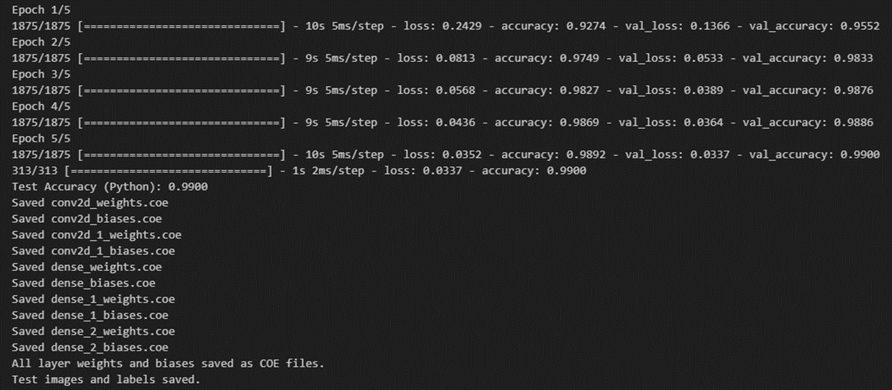
Python에서 확인한 정확도는 99%로,
실제 다른 경우에서는 이정도 정확도를 가지기 어렵지만
학습용 데이터를 사용하였기 때문에 가능합니다.
- FPGA 정확도
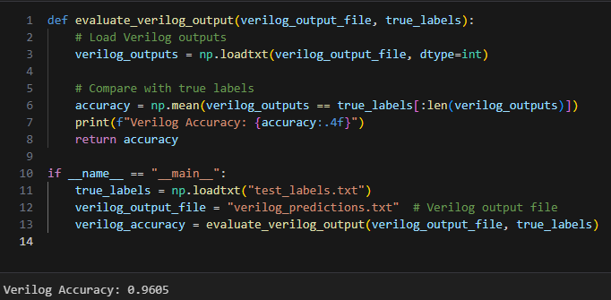
FPGA에서 나온 예측값들의 정확도는 96%로,
앞서 8bit fixed point로 구현하면서 타협봤었죠.
모델의 성능 차이는 3% 내외로 준수한 성능을 보입니다.
다른 경우에서는 Domain에 따라 어느 정도까지 타협을 볼지 정해야겠지만,
장비의 memory를 생각하며 먼저 python으로 성능을 테스트 한 뒤에
FPGA에 그 모델을 구현해서 칩에 AI를 구성할 수 있습니다.
'RTL, Synthesis, P&R' 카테고리의 다른 글
| Filter - (1) 2차원 Filter (0) | 2024.09.09 |
|---|---|
| Cortex-M0 SOC 활용 - (3) Snake game with API (0) | 2024.09.09 |
| Cortex-M0 SOC 활용 - (2) Peripheral with C,CMCIS (0) | 2024.09.09 |
| Cortex-M0 SOC 활용 - (1) AMBA3 AHB-Lite와 Pheripheral (0) | 2024.09.09 |
| 16KB Cache Memory Controller - (1) RTL 및 Coverage (0) | 2024.09.07 |